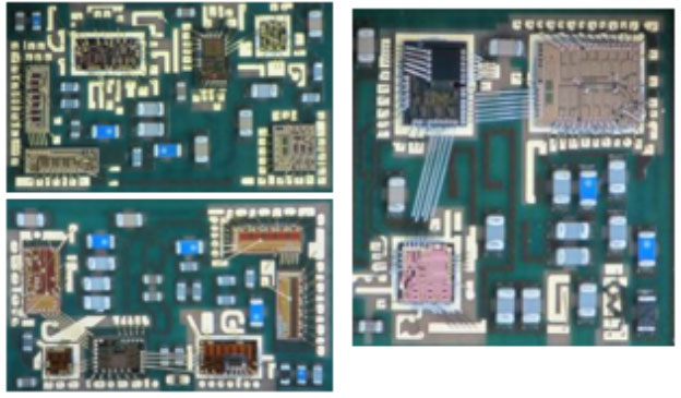
Carsem’s SiP (System in Package) is the advanced technology of placing multiple ICs and passive components into a single package. Our services include design, modeling as well as final test including RF testing of Bluetooth and WLAN applications.
Features
- Package construction : Leadframe and laminate based
- Package size up to 12×12 mm
- Terminal Pitches as fine as 0.4mm
- Package Thickness from 0.5 mm to 2.5 mm
- Flip chip, wire bond and stacked die capabilities
- Ability to mount passive components as small as 01005
Applications
There is an almost endless list of potential SiP applications and some examples are :
- Bluetooth TM
- Wireless Devices
- 802.11 WLAN Applications
- Power Management Devices
- RF Power Amplifier
- GPS Modules
- Internet Mini-Systems
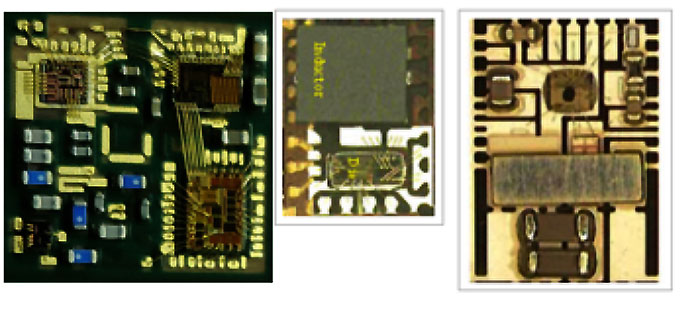
SiP LGA
SiP (System In Package) LGA is a package that consist of a combination of dies, passive components, or shielding in an IC package format. The connection of silicon die to package can be in the form of wire-bond or flip chip.
Applications
SiP LGA package is one of the most commonly industry standard packages. SiP is commonly used logic, memory, micro-controllers, automotive consumer and communications products. Such as RF Power Amplifier, GPS (Global Positioning System), and Power modules.
RF Power Amplifier
Product Feature
- GaN or GaAs wafer
- Multi die integrate in one package
- Critical WB parameter control
- Various components
Applications
Different frequency range for 4G/5G power amplifier production apply on smartphones.
GPS (Global Positioning System)
Product Feature
- Multi die integrate in one package
- Various components
Applications
Widely used in automotive consumer and smartphones.