A Trusted & Proven MEMS Partner
Carsem is a global leader in MEMS & Sensors advanced packaging & test and is among the world’s leaders in microelectronics packaging.
Carsem has a dedicated MEMS & Sensors Business Unit (MSU) which drives focused investments in this area. MSU boasts of “advanced design, development & prototyping capabilities” to accelerate MEMS products towards mass manufacturing. By virtue of a strong automotive MEMS sensor portfolio, MSU’s emphasis on Quality continues to inspire customer’s confidence in its capabilities to launch new sensor packages in a variety of applications including Industrial, IoT, and Consumer segments.
Turnkey MEMS & Sensor Services
Our dedicated and experienced MEMS Team can provide comprehensive turn-key solutions that begins with package co-design, thermal/stress simulations, engineered BOM selection for reliability, qualification support and in-house test development.
Package Offerings
ENVIRONMENTAL HUB MEMS SENSORS PACKAGE OVERVIEW
- Custom Molded Cavity Packages
- Lid packages with metal and plastics (LCP)
- Laminate and lead-frame base packages
INERTIAL HUB MEMS SENSORS PACKAGE OVERVIEW
- SOIC family
- QFN / DFN & Micro Leadframe Packages (MLP)
- LGA (LF, MIS) and Custom Packages
MAGNETIC & CURRENT HUB MEMS SENSORS PACKAGE OVERVIEW
- SOIC family
- LGA (MIS) and Custom Packages
Types of Packaging Solution within MEMS & Sensors:
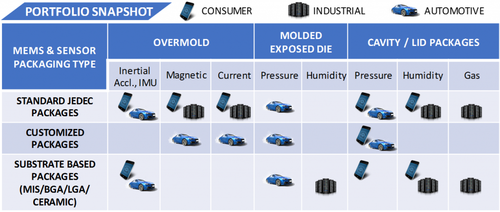
Carsem MEMS Sensors Business Unit Product Portfolio
Carsem Advantage
EXPERIENCED MEMS STAFF
- A Fully Dedicated MEMS Staff
- History of Launching Difficult MEMS Sensors
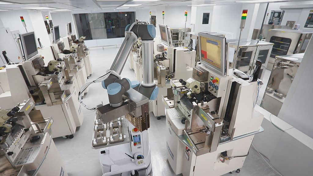
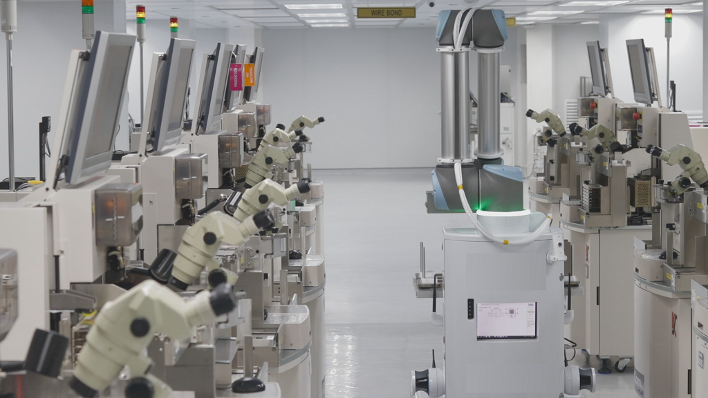
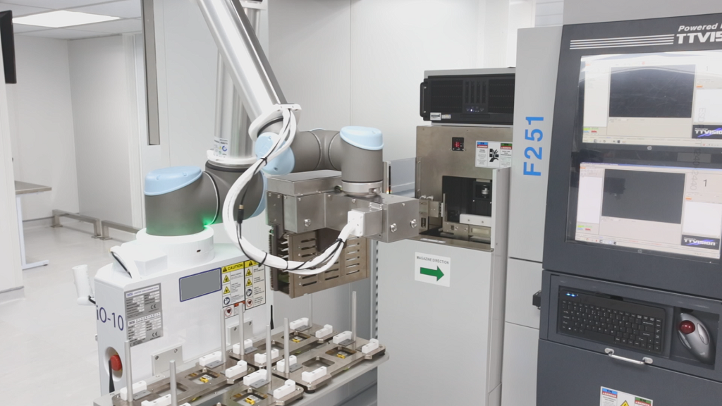
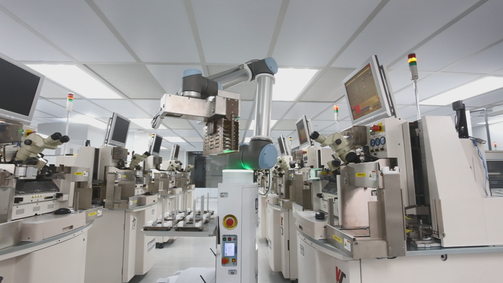
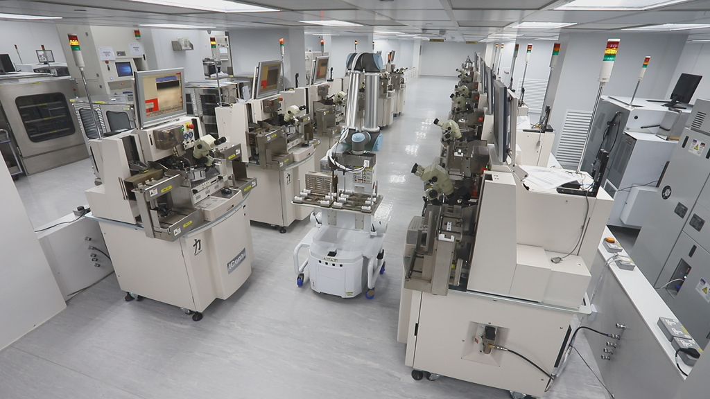
DEDICATED MEMS MANUFACTURING LINES
- Dedicated MEMS Manufacturing Line
- IATF 16949, ISO-9001, ISO-14001, ANSI/ESD
- Investment in the latest Equipment
- State-of-the-Art Industry 4.0 Assembly
- Manufacturing Excellence System (MES)
- Complete traceability and data analytics
ADVANCED CORE TECHNOLOGY & TOOLBOX
- Cutting Edge MEMS Packaging Roadmap
- Advanced Electronics Materials Roadmap
- Advanced MEMS Wafer & Die Preparation
- Advanced MEMS Die Bond & Wirebonding
- Advanced Molding Technology for MEMS
- System in Package (SiP) Technology
- Flip Chip and CuPillar Technology
- Molded Interconnect Substrates (MIS)
SIMULATION, ANALYSIS, AND DESIGN OPTIMIZATION
- Thermal-Mechanical Simulation
- Electrical Simulations
- RF Simulation
- Mold Flow Simulation
- For Package & Board Level Reliability
Availability
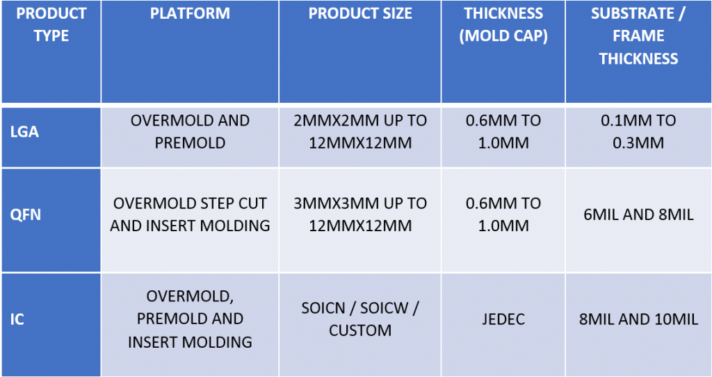
1) Packages : LGA / MIS from 2mmx2mm to 10mmx10mm
- Mold cap: 0.52mm – 1.2mm
- Substrate thickness: 120um – 320um
- Capability integration with SMT from 0201, 0402 and 0603
2) Packages : MLP from 2mmx2mm to 10mmx10mm
- Mold cap: 0.52mm – 1.2mm
- Lead frame thickness: 150um to 200um
3) Customized Cavity package and Over mold packages on substrate and lead frame
The packages performance depends on customer requirements from MSL, MSL2 , MSL 3 to Automotive Grade 0 to 3.