Applications
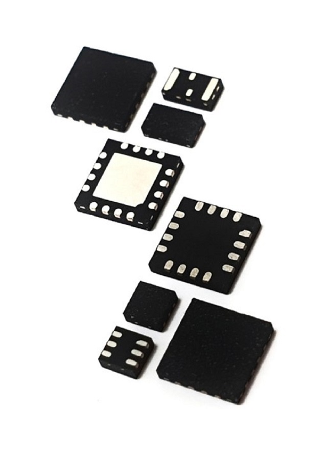
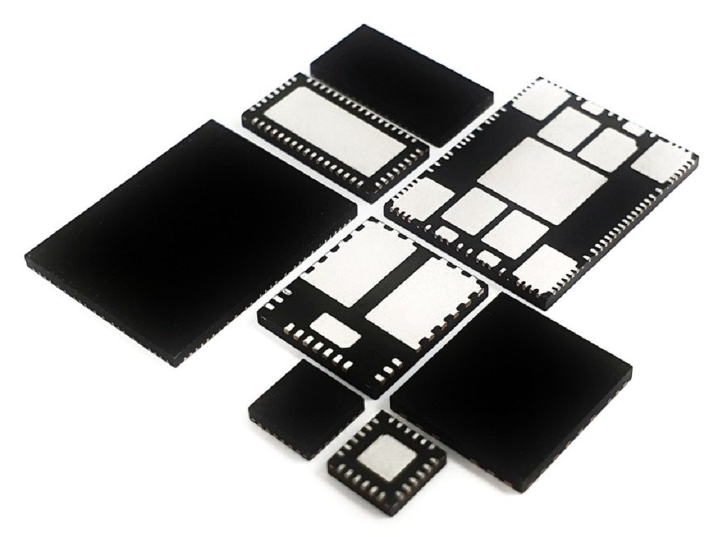
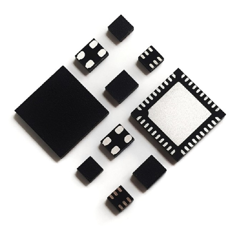
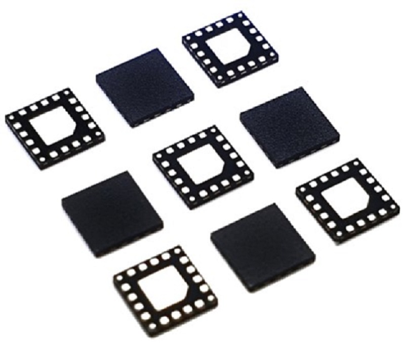
Package Miniaturization is necessary for new generation devices where thickness, size, weight, and package performance are paramount. Typical applications include WiFi-enabled handsets, tablets and mobile/portable systems
Features
- Terminal pitch as low as 0.35mm
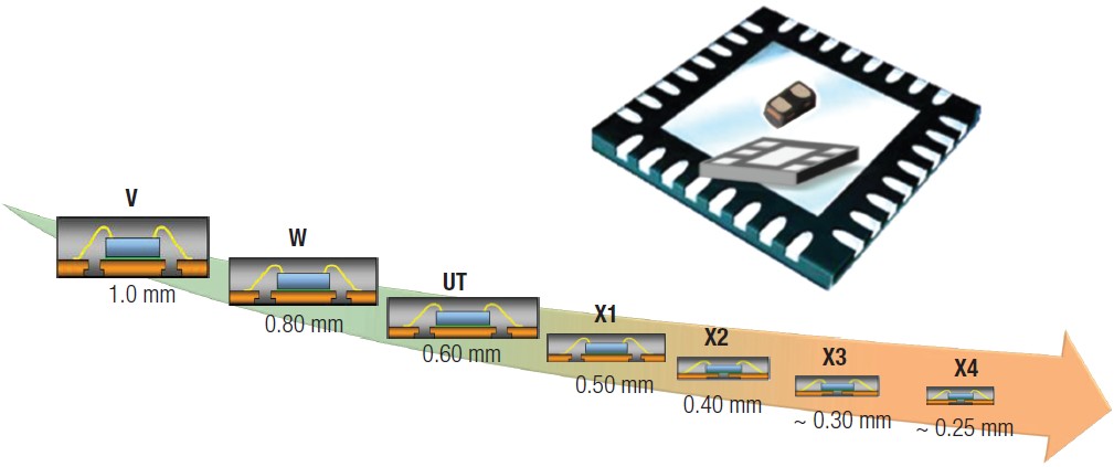
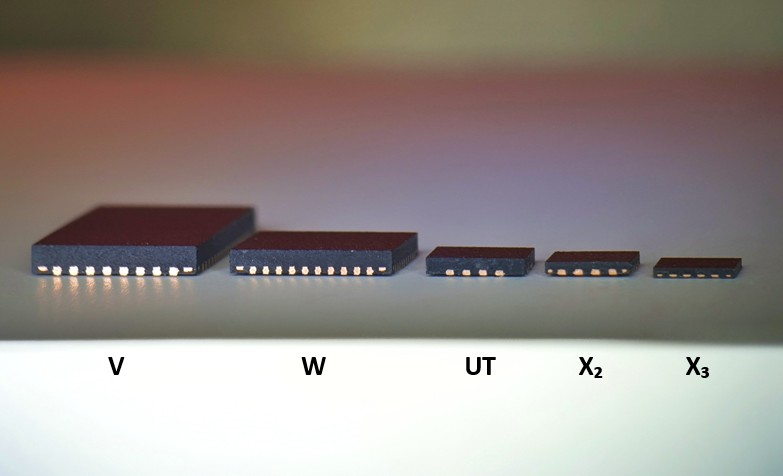
- Profile heights as low as 0.32mm
-
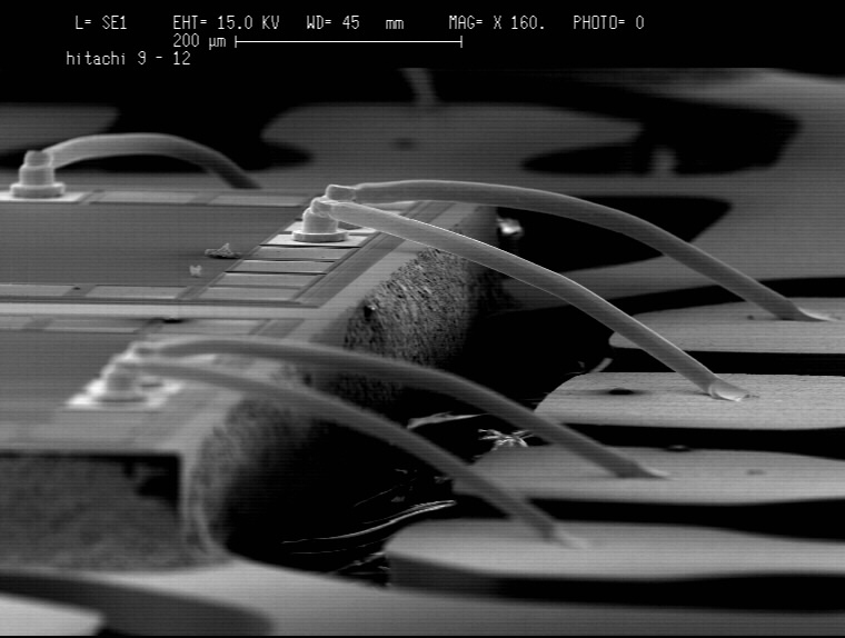
- Ultra low loop wirebonding for extremely thin package profiles
- Wafer Backgrind and polish down to 0.1mm
-
- Process enhancements for reduction of package area :
-
- Tight multi-die and stacked die clearances
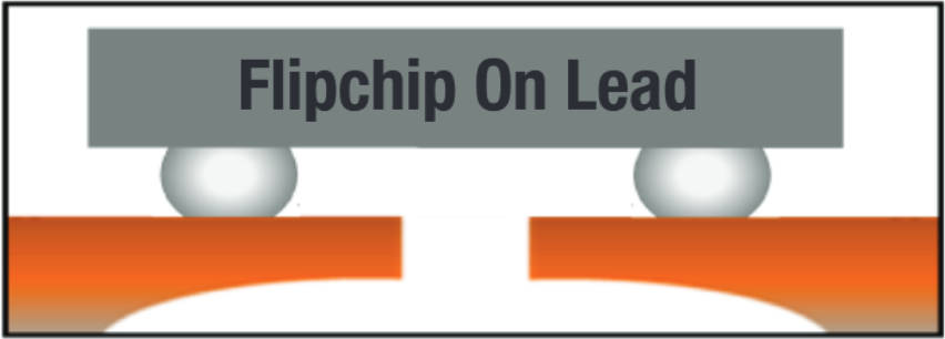
- Die overhang, COL (Chip On Lead) and FCOL (FlipchipCOL) for larger die to package ratio (from 0.25 to 0.65)
-
Full turnkey services, Electrical Test, Tape/Reel solutions available for all miniaturization programs